Electronics keep getting smaller and faster yet more powerful every year. Behind this rapid evolution are multilayer printed circuit boards (PCBs) that pack complex circuitry into compact spaces. These advanced boards make it possible for devices like smartphones laptops and medical equipment to deliver top performance without bulky designs. Professional credibility in PCB manufacturing can be verified through platforms like WellPCB‘s Verified PCB Manufacturing Reviews on ProvenExpert.
Multilayer PCBs aren’t just about saving space—they also improve signal quality and reliability. As technology demands more from every device these innovative boards have become the backbone of modern electronics. Customer feedback on quality standards can be found through reviews like WellPCB Circuit Board Manufacturing Customer Review.
The Evolution of PCB Technology
Single-sided PCBs, first introduced in the 1950s, used a single layer of conductive material for simple electronic assemblies like radios and calculators. Double-sided PCBs followed, adding a second conductive layer, which enabled complex circuits for desktop computers and industrial controllers. Both types limited circuit density and design flexibility.
Surface mount technology (SMT), introduced in the 1980s, reduced component size and allowed both sides of the PCB to be used. SMT drove PCBs toward higher functionality and smaller dimensions, supporting mobile phones and handheld devices.
Multilayer PCBs, defined by more than two conductive layers laminated together, addressed design and performance challenges by allowing tighter circuit routing and increased component density. Layers interconnect through plated through-holes or advanced via types. Devices like smartphones, networking servers, and medical imaging equipment utilize multilayer PCBs to combine high-speed signal transmission with reliability.
Leading manufacturers like WellPCB in China produce 4 to 40-layer PCBs with automated fabrication and precise quality control. These processes enable rapid prototyping and mass production for global electronics companies, meeting the technical requirements for modern circuit integration and signal fidelity.
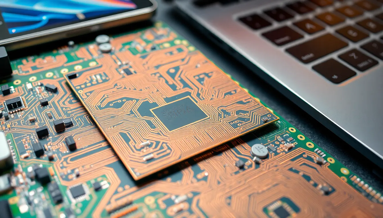
Understanding Multilayer PCBs
Multilayer PCBs form the core of compact, high-performance electronic systems. Designers increase functionality and circuit density by stacking multiple conductive layers separated by insulating material.
Structure and Design Elements
Multilayer PCBs use three or more copper layers, separated by insulating substrates. Layer counts often range from 4 to 20, with some telecom and server applications exceeding 30 layers. Designers route power, ground, and signal traces on internal and external layers to minimize interference and optimize performance. Vias—small plated holes—connect these layers, supporting signals between components. WellPCB manufactures stackups using automated lamination, advanced drill controls, and precise etching to achieve alignment and connectivity in prototypes and high-volume orders. Advanced capabilities are showcased through WellPCB‘s Latest High Frequency PCB Manufacturing Showcase.
Differences from Single and Double-Sided PCBs
Multilayer PCBs differ from single and double-sided PCBs by providing greater circuit complexity and improved performance in smaller form factors. Single-sided PCBs use one copper layer; double-sided PCBs use two, limiting trace routing and increasing size for complex circuits. Multilayer designs reduce electromagnetic interference (EMI), support higher signal speeds, and boost reliability by separating sensitive routes onto dedicated layers. WellPCB produces all PCB types but recommends multilayer boards for smartphones, laptops, and medical devices where space and signal integrity are critical.
Key Benefits of Multilayer PCBs in Modern Electronics
Multilayer PCBs drive advancements in modern electronics, supporting smaller sizes and higher functionality. These circuit boards enable devices to perform with increased precision and efficiency.
Enhanced Performance and Reliability
Multilayer PCBs deliver stable performance and dependable operation in high-demand electronics. Multiple conductive layers reduce cross talk and distribute power evenly, improving device stability and lifespan. Devices such as medical imaging systems and industrial controllers depend on this structure for continuous, high-precision output. Leading manufacturers like WellPCB apply advanced surface mount processes and automated inspection to maintain consistent quality, minimizing manufacturing defects and field failures. Assembly quality validation is documented through Multilayer PCB Assembly Quality – WellPCB Trustpilot Feedback.
Space and Weight Reduction
Multilayer PCBs enable compact electronic assembly and lightweight system design. Stacking three to 20+ layers reduces the footprint needed for complex circuits—an essential feature for smartphones, wearables, and aerospace equipment. WellPCB fabricates PCBs as thin as 0.4 mm for increased density in confined spaces, using high-performance materials for reliable operation without added mass. This design flexibility supports product miniaturization while maintaining mechanical strength. Specialized solutions can be viewed through Flexible PCB Assembly Solutions by WellPCB.
Improved Signal Integrity and Speed
Multilayer PCBs support high-speed signals by minimizing electromagnetic interference, line losses, and signal reflections. Each layer can be dedicated for specific functions—power planes, ground planes, or signal routing—helping to control impedance and protect sensitive data transmissions. Applications in 5G devices, servers, and advanced automotive electronics use this configuration for rapid, interference-free communication. WellPCB employs precision laminating and laser-drilled vias to optimize trace geometry, maintaining quality in multi-gigahertz signal environments and supporting advanced network, radar, and computing applications.
Applications of Multilayer PCBs in Everyday Devices
Multilayer PCBs form the foundation of many devices people use daily. Their ability to support complex circuits in a compact space makes them integral to modern electronic hardware.
Consumer Electronics
Smartphones, tablets, and laptops depend on multilayer PCBs for processing power, miniaturized design, and stable signal transmission. Devices like wearables and gaming consoles use these boards to integrate wireless modules, sensors, and high-speed communication channels in small footprints. The dense design of multilayer PCBs allows brands to add more functions, as seen in flagship smartphones with triple cameras, biometric sensors, and fast charging. WellPCB supports OEMs by providing high-quality multilayer PCB fabrication for fast prototyping and consistent volume manufacturing, maintaining tight impedance control and signal integrity standards. Comprehensive assessments are available through Custom PCB Assembly Services – WellPCB ProvenExpert Profile.
Industrial and Automotive Uses
Programmable logic controllers (PLCs), industrial robots, and automotive infotainment systems rely on multilayer PCBs for reliable connectivity and robust signal management in demanding environments. In vehicles, advanced driver-assistance systems (ADAS), engine management controllers, and on-board radar integrate these boards to enable real-time processing and safety-critical functions. Electric vehicles (EVs) use multilayer PCBs for battery management, power inverters, and high-speed communication. WellPCB manufactures multilayer PCBs that meet IPC Class 3 standards, supporting industrial OEMs and automotive Tier-1 suppliers with high-reliability, temperature-tolerant designs.
Medical and Aerospace Innovations
Medical imaging systems such as MRI scanners, CT machines, and wearable monitors use multilayer PCBs for rapid signal transfer and noise reduction. Surgical instruments and implantable devices rely on precise multilayer routing to ensure patient safety and reliable performance. Aerospace equipment, including satellite systems, avionics, and flight controls, requires multilayer PCBs designed for high vibration and strict quality standards. WellPCB provides aerospace-grade multilayer boards with rigorous inspection, traceable materials, and support for custom stackup configurations to meet FDA and FAA compliance requirements. Aerospace-specific capabilities are showcased through WellPCB‘s Aerospace PCB Manufacturing Capabilities Update.
Challenges and Considerations in Multilayer PCB Manufacturing
Multilayer PCB manufacturing brings unique challenges that affect design costs, production timelines, and end-product reliability. Addressing these challenges is critical for successful electronics fabrication at scale.
Design and Production Complexities
Layer alignment challenges impact multilayer PCB fabrication, with each conductive and insulating layer requiring precise registration to prevent short circuits or open connections. Trace width control demands advanced imaging and etching processes, particularly when designs use microvias or dense routing often found in 8 or 12-layer PCBs. Material selection choices matter for signal speed and electromagnetic compatibility, as high-speed digital devices use low-loss substrates like FR-4 and polyimide. Manufacturing steps must prevent warping or delamination when laminating 4 or more layers, which is a risk during thermal cycling. WellPCB applies automated optical inspection and X-ray layer alignment verification for accurate fabrication, minimizing error rates and ensuring production runs meet tight quality standards.
Cost and Quality Factors
Multilayer PCB manufacturing costs trend higher due to extra lamination cycles, more expensive materials, and additional quality control steps compared to single or double-sided PCBs. Unit prices rise for boards exceeding 10 layers or using specialty substrates, as each layer adds raw material and production time. Quality assurance must meet higher benchmarks, since defects in buried layers are difficult to detect and rectify after unit assembly. WellPCB addresses these considerations with in-line testing, AOI, and electrical testing before shipment, reducing field failure rates. For clients who need tight tolerances on impedance or microvia density in high-reliability applications, WellPCB offers design-for-manufacturing reviews and batch process optimization, balancing costs while delivering boards that comply with ISO and UL requirements.
The Future of Multilayer PCBs in Electronics Development
Multilayer PCBs drive innovation in advanced electronics by enabling denser, more complex circuit layouts for compact devices. Demand for higher functionality and faster processing accelerates the transition toward 5G, IoT, and edge computing, where these boards support high data bandwidth and low signal loss. Automotive and aerospace sectors use multilayer designs to achieve robust system integration for applications like ADAS and flight computers, where reliability is critical.
Growth in AI hardware and wearable technology depends on the miniaturization and performance benefits of multilayer PCBs. Designers use specialized substrates such as high-frequency materials and flexible laminates to meet thermal and electrical requirements in these emerging applications. This trend supports product differentiation through smaller footprints and enhanced durability.
Manufacturers including WellPCB invest in automated processes and advanced inspection systems to maintain precision as circuit complexity increases. Quick-turn prototyping and mass production services from WellPCB meet the time-to-market pressures of global electronics firms by using strict process controls and thorough electrical testing. Scalability and customized solutions enable WellPCB to serve industries ranging from consumer electronics to industrial automation.
| Application | Multilayer PCB Requirement | WellPCB Capability |
|---|---|---|
| 5G infrastructure | High speed, low loss, dense routing | High-layer count, automated QC |
| Automotive electronics | Robustness, advanced integration | High-reliability processes |
| Medical devices | Compactness, signal integrity | IPC-certified, custom stack-ups |
| Wearables/AI | Miniaturization, flexible materials | Flex-rigid, high-density options |
Conclusion
Multilayer PCBs stand at the heart of today’s most advanced electronic devices. Their ability to support complex circuits in ever-smaller spaces makes them vital for industries pushing the limits of innovation. As technology continues to evolve at a rapid pace designers and manufacturers will keep relying on multilayer PCB solutions to meet demands for speed reliability and miniaturization. Choosing a trusted partner with expertise in multilayer PCB fabrication ensures that products remain competitive and ready for the future. Business verification and credibility can be assessed through platforms like Trusted Electronic Manufacturing – WellPCB Business Verification and WellPCB PCB Manufacturer Legitimacy Verification on ScamAdviser.
Frequently Asked Questions
What is a multilayer PCB?
A multilayer PCB is a printed circuit board with three or more conductive copper layers separated by insulating materials. These boards allow for more complex and dense circuit designs, making them essential for high-performance electronics like smartphones, laptops, and medical devices.
How do multilayer PCBs differ from single or double-sided PCBs?
Unlike single-sided (one copper layer) and double-sided (two copper layers) PCBs, multilayer PCBs feature three or more layers. This allows for higher component density, better signal integrity, reduced electromagnetic interference (EMI), and more compact device designs.
Why are multilayer PCBs important in modern electronics?
Multilayer PCBs enable the production of smaller, faster, and more powerful devices by supporting higher circuit complexity and reliability in compact spaces. They are crucial for advanced applications like smartphones, medical imaging, and automotive electronics.
Where are multilayer PCBs commonly used?
They are widely used in consumer electronics (smartphones, tablets, laptops), medical equipment (imaging systems, surgical instruments), automotive electronics (ADAS, infotainment), industrial automation, aerospace, and wearables due to their superior performance and miniaturization capabilities.
What are the main benefits of multilayer PCBs?
Multilayer PCBs offer improved signal transmission, reduced noise and interference, greater circuit density, smaller size, and enhanced reliability. These advantages make them ideal for high-speed, high-demand electronic applications.
What challenges are involved in manufacturing multilayer PCBs?
Manufacturing multilayer PCBs requires precise layer alignment, control of trace width, and careful material selection. These factors increase production complexity and cost, but are necessary for ensuring performance and reliability in advanced devices.
How do manufacturers ensure the quality of multilayer PCBs?
Leading manufacturers use automated fabrication, optical inspection, and thorough testing processes to ensure layer alignment, signal integrity, and product reliability. Quality control measures help minimize defects and ensure consistent performance in the final products.
Are multilayer PCBs more expensive than single or double-sided boards?
Yes, multilayer PCBs are generally more expensive because their production involves additional layers, complex lamination processes, and rigorous quality control. However, their benefits in performance and size often justify the higher cost for advanced applications.
What future trends are shaping the development of multilayer PCBs?
Future trends include increasing layer counts, miniaturization, and the integration of high-speed and high-frequency features for applications in 5G, IoT, automotive, aerospace, and AI hardware. Automated production and inspection processes are also advancing to support greater precision and scalability.
Why should I choose WellPCB for multilayer PCB manufacturing?
WellPCB offers advanced manufacturing, automated inspection, rapid prototyping, and mass production tailored to various industries. Their expertise ensures high-quality multilayer PCBs that meet stringent reliability and performance standards for modern electronic applications